The very nice thing about making a project that’s just for us to use (as opposed to a product we’d like to sell) is that we can take bits of people’s hardware designs and/or code and use it with abandon – or at least without having to worry about a potential copyright violation. In this particular post we’re going to go over how to run the code examples ST provides for interfacing with their eval board hardware and look at the code for their LTDC paint example, which may become the foundation upon which we do the drawing of elements on our screen for this oscilloscope.
As I’ve mentioned before, ST maintains a collection of examples and “applications” called STM32CubeF4 that showcases the capabilities of the microcontroller when it is connected to the different components on the evaluation board. Here you will find anything from small snippets of code going over how to set up a timer to full-blown applications like LTDC Paint which emulates a simple “MS Paint”-like program on the display (LTDC stands for “LCD TFT Display Controller”, where “LCD” and “TFT” are their own acronyms).
Some of the Cube examples are simple or focused enough that the only thing we’d like to do with them is look at the code to see how something works (like setting up a timer or playing around with interrupts). The applications, however, are more or less full-fledged ideas that we’d like to run on the board and interact with. ST provides the source-code for everything without the binaries, so first we have to figure out how to set up and build the project on SW4STM32. Let’s delve on how to do this first.
Building and Running STM32CubeF4 Projects
I’m a little embarrassed to admit that it took me about an hour and a half to figure out how to do this – I know that because I had just configured my bread machine to knead and rise a pizza dough for me and that’s how long that process takes. In my defense, the STM32CubeF4 folders are set up in a way that makes them look like you’re just supposed to open up a project inside of them and have it all magically work…
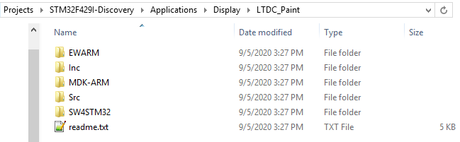
Anyway, let’s go ahead and set up the LTDC Paint example step-by-step so that we can run it. Below you’ll see a screenshot of the folder corresponding to this example inside the STM32CubeF4 directory (Projects/STM32F429I-Discovery/Applications/Display/LTDC_Paint):
If you’re like me, you’ll see the Inc and Src folders and think all you have to do is start a new SW4STM32 project in here (or in a copy of this directory) and then link it all together inside of Eclipse somehow. That is absolutely not the way to do it. The problem with this approach is that this folder is not all there is to this project – it uses code from the Utilities folder all the way up at the root of the STM32CubeF4 directory, and the correct linking for all these files is in the “SW4STM32” folder of the LTDC_Paint application.
Here’s the process for getting this or any other project loaded into ST4STM32 correctly. Open up the IDE in your preferred workspace (it does not have to be where you have the STM32CubeF4 files stored) and select File->Import. A submenu will open from which you should select “Existing Projects into Workspace” under “General.” In the next window, select the SW4STM32 folder (not the LTDC_Paint directory) as the root directory (for example, Projects/STM32F429I-Discovery\Applications\Display\LTDC_Paint\SW4STM32). Once you do that, “STM32F429I-Discovery” should show up as an option (side-note: this means you can’t already have a project in your workspace called “STM32F429I-Discovery,” which is kind of annoying since they’re all called that…if you do, just remove it and start over). It may be a good idea to select “Copy projects into workspace” to create a copy to leave their example untarnished, but you can also download the example again if something happens.
[It’s probably good to mention here – do not rename the projects to something other than STM32F429I-Discovery – it’ll break how the files are linked and changing it back will not fix it! If you run into this, just download the files again from ST’s site, or figure out a way to fix it and let me know!]
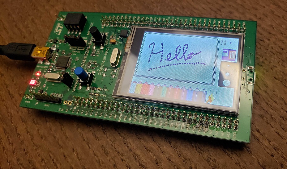
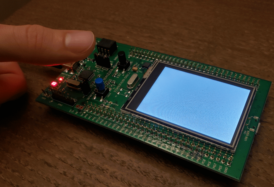
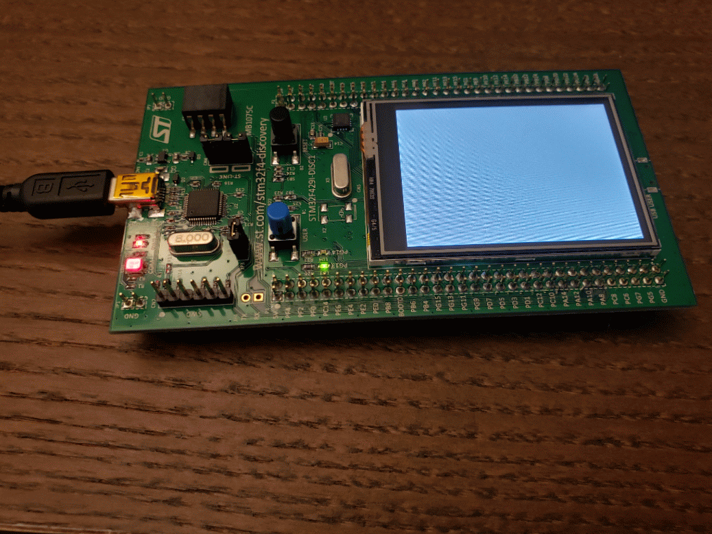
At this point, you can hit “Finish” and you should have a new project in your workspace (or linked to it from elsewhere) called STM32F429I-Discovery” which you can build and try out. In this case, “LTDC Paint” is a MS-paint-like program that runs on the LTDC touchscreen (by the way: the code is under the “Example” folder):
ST’s LTDC_Paint application running on my evaluation board
That’s great, but what does this do for us?
Well, we can use ST’s code as a template for all the drawing to screen we need to do for our oscilloscope, from text that shows our trigger level and cursor settings to the dots that make up the waveform we want to show the user. The functions in LTDC_Paint help abstract certain aspects of how the DRAM and display work, so that all we have to do is call functions such as:
Function
Description
BSP_LCD_DisplayOn()
Initializes the display
BSP_LCD_Clear(COLOR)
Clears the display and draws a solid background of the color provided
BSP_LCD_FillRect(x, y, width, height)
Draws a filled rectangle of specified width and height at position (x, y)
BSP_LCD_DisplayStringAt(x, y, text, mode)
Draws some text at (x, y)
Some examples of useful functions implemented in LTDC_Paint
There are also some very helpful definitions of fonts and color configurations which we can copy and use as we wish!
We can similarly take other bits and pieces of code from ST’s applications and examples to get the functionality we want for timers, interrupts, and other processor configuration code we’ll need. For the next update, I’ll attempt to modify the LTDC_Display code to display some axes and other simple display elements we’ll need on the oscilloscope screen. Stay tuned for this and, soon after it, some initial work on building the triggering circuitry from logic gates; you know I can’t have too many consecutive posts about software – I am a hardware engineer, after all!
Today we’ll continue to play with the STM32F429-DISC1 eval board to learn more about the MCU and what it can do.
What’s an interrupt?
If your childhood was anything like like mine, your parents probably reprimanded you whenever you interrupted someone while they were talking. And if you were anything like me, you were interrupting because something occurred to you (likely as a response to whatever was being said by the interrupted person) and you wanted to say it before you forgot what it was, or maybe before it lost its impact.
Like us humans, the processor inside an MCU is in an environment with lots of action going on around it – buttons connected to it are being pressed, samples are coming in from an ADC, memory is filling up, timers are going off, and all sorts of other things are happening. There are two common ways of dealing with all this action – let’s review them real quick.
One approach, which as you’ll recall we used on the nixie clock project and is described here, is called polling. In a polling architecture, the processor checks on its subsystems “once in a while” to see what happened; the processor will set its own “checking periods” and is responsible for spending that time looking at each subsystem to see if it has anything to report to it. Some subsystems will have flags (bits that are set or cleared) that tell the processor that something happened since the last time that it checked; the error counters inside of Ethernet PHY chips are good examples of this – many error counters are self-clearing and the processor is expected to check them every once in a while. Other subsystems are not this smart – GPIO pins connected to buttons are either high or low, and if you’re not polling quickly enough you might just miss something that happened (e.g. you may only register one button press if there were two quick button presses in succession). Polling has fallen out of favor because, although it is simpler from an architecture, “wrapping your head around it” point of view, it is also more processor intensive. This is because the processor can’t be in “sleep mode” as much, as it has to constantly be waking itself up to check all the subsystems. In a battery-powered product, for example, you’d ideally like the processor to be asleep as much as possible, waking up only when absolutely necessary to deal with something that’s happened (like a button press).
This is where the second approach comes in, and that’s interrupts. Most processors have an interrupt controller built in to it, and that interrupt controller is connected to a wide variety of interrupt sources (both internal and external to the MCU). Here’s some examples:
GPIO pins connected to external devices (control signals, buttons/keypads, etc.)
Internal timers that can be configured to generate an interrupt every so often
Specific bits inside of registers that indicate various states for internal subsystems (e.g. a “half-full flag” inside a FIFO memory telling you that it’s now half full, a “link bit” inside an Ethernet PHY that tells you that a cable was plugged-in, an “enumeration complete” bit inside a USB or PCIe controller register that tells you a new device was hooked-up)
And more!
You have to write code to set up the interrupts – this means you want the interrupt controller to pay attention to the interrupts you specify in particular (the controller will typically ignore all sources by default). You can configure specific details about the interrupt source – like whether you want it to interrupt when the GPIO pin goes high only, or low only, or both when it goes high and low (for an edge-triggered interrupt). Then you register an interrupt handler function, which is the function that gets called whenever an interrupt of that type is received. Finally, you assign a priority to the interrupt – this is important because some interrupts will fire when you’re halfway through dealing with an interrupt, and in some cases you want to set that aside for a moment, deal with the new interrupt first, and come back to the old interrupt. And in other cases you most certainly do not want to do that.
Here’s a short example of why the priority is important. Let’s say we have two interrupt sources, one is connected to GPIO pin 0 of bank A, which is a push-button, and the other is an internal timer which we configured to fire every 10 ms to keep track of time. The interrupt handler for the button increments a variable in the code which represents how may times the button has been pushed. The interrupt handler for the timer adds 10ms to a variable which represents a supposedly accurate counter of how long it has been since the program started. The board has a display which shows both the time since the program started and the button-press counter. In this simple example, we’d like to have the timer interrupt have higher priority than the button interrupt because we’d like the time variable to be as accurate as possible. It doesn’t hurt anything if it takes a few extra milliseconds to update the button counter because the program was in the middle of doing that when the timer interrupt arrived. However, if we wait for the button interrupt to finish first (if they have equal priorities or if the timer priority is lower), then we’ll have an inaccurate time variable for the rest of the program’s length!
The important thing to keep in mind with interrupts is that we’re handing over the control of when the code gets called to the processor. When we write code for a polling-based architecture, we know exactly when and how often each subsystem gets polled (as a consequence, we might be responsible for writing the code poorly so we end up missing some events, but we still know when the checks happen). With interrupts, we write code that ends up looking a little more disjointed – instead of our main loop being a step-by-step procedure where we, for example, check a button, increment at timer variable, and write these two to the display, all we do in it is write the variables to the display and call it good; instead, somewhere else in the code there’s these two functions that look like they never get called from the main loop but are responsible for incrementing the variables. The processor is then responsible for bringing these two pieces of code together so that they do what we want them to do. Priority, masking, and some other things that we set up at the beginning of the program tells the processor how to do so to get the behavior that we want from the program.
A simple example
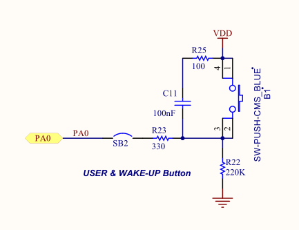
In this example we’ll set up an interrupt on the eval board’s blue push-button switch (the black one is a reset button, so we can’t use it in the code) that will toggle the LED on and off. Here’s the schematic for it:
Pushbutton schematic on the Discovery board
Note that the button is already debounced in hardware (via R25, C11, and R23) and the signal goes high when the button is pushed. It is connected to pin 0 of GPIO bank A. You’ll remember from the previous post that the green LED is connected to pin 13 of GPIO bank G. So here’s what we have to do to get the behavior we want:
Initialize GPIO bank G as we did before (to output on both the green and red LED)
Write an interrupt handler that toggles the LED pin (that’s all it has to do, ST’s code deals with clearing the interrupt and all the other “gritty embedded stuff” for you)
Initialize GPIO bank as an input with interrupt capability on pin 0. We’ll set it up so it’s edge-triggered when the signal transitions from low to high. The priority can be almost anything since it’s the only interrupt we’ll write; let’s keep it low to make sure nothing else breaks. Finally, we have to tell the processor that the function we wrote above is the interrupt handler for this interrupt.
That’s it! The while loop can just be an infinite loop that does nothing so that the program keeps running rather than just ending.
You can go ahead and write a program like we did in part 3 of the series. You can copy the clock configuration (SystemClock_Config) and error handler (Error_Handler) functions from there. Here’s our main loop, which will be very similar to the one from that post:
#include "stm32f4xx.h"
#include "stm32f429xx.h"
#include "stm32f4xx_hal_gpio.h"
#include "stm32f4xx_hal.h"
#include "stm32f4xx_hal_exti.h"
#include "stm32f4xx_it.h"

static void SystemClock_Config(void);
static void Error_Handler(void);
static void EXTILine0_Config(void);

int main(void)
{
    // Initialize the hardware abstraction layer libraries
    HAL_Init();
    __HAL_RCC_GPIOG_CLK_ENABLE();

    GPIO_InitTypeDef g = {GPIO_PIN_13 | GPIO_PIN_14, GPIO_MODE_OUTPUT_PP, GPIO_NOPULL, GPIO_SPEED_FREQ_LOW};
    HAL_GPIO_Init(GPIOG, &g);

    /* Configure the system clock to 180 MHz */
    SystemClock_Config();

    /* Configure EXTI Line0 (connected to PA0 pin) in interrupt mode */
    EXTILine0_Config();

    while (1) {

    }
}
Note that the main difference is that we now have a EXTILine0_Config() function which will configure an external interrupt (I guess that’s what “EXTI” is) on line 0 (the button) of GPIO bank A. That looks like this:
/**
  * @brief  Configures EXTI Line0 (connected to PA0 pin) in interrupt mode
  * @param  None
  * @retval None
  */
static void EXTILine0_Config(void)
{
  GPIO_InitTypeDef   GPIO_InitStructure;

  /* Enable GPIOA clock */
  __HAL_RCC_GPIOA_CLK_ENABLE();

  /* Configure PA0 pin as input floating */
  GPIO_InitStructure.Mode = GPIO_MODE_IT_RISING;
  GPIO_InitStructure.Pull = GPIO_NOPULL;
  GPIO_InitStructure.Pin = GPIO_PIN_0;
  HAL_GPIO_Init(GPIOA, &GPIO_InitStructure);

  /* Set EXTI Line0 Interrupt to the lowest priority and enable the interrupt */
  HAL_NVIC_SetPriority(EXTI0_IRQn, 2, 0);
  HAL_NVIC_EnableIRQ(EXTI0_IRQn);
}
A lot of this looks the same as the GPIO bank G initialization. Note that the “mode” parameter of the structure is now set to GPIO_MODE_IT_RISING, which will be an input that issues an interrupt on a rising edge. Finally, we set the priority to 2 (on a scale from 0 to 15, where 0 and 1 are really low priority events we shouldn’t mess with) and the subpriority to 0 (I’m not sure what that is yet, if we’re being honest), and the interrupt (often shortened to “IRQ”) is enabled. A few other things to note – internally, all the GPIO banks are connected together, so that all pin 0s (of bank A, bank B, all the way to bank G) can only issue EXTI0_IRQn interrupts. That’s something we’re going to have to keep in mind. That’s why pin 0 of bank A (the one that the button is connected to) corresponds to EXTI0_IRQn. It also means that ST has configured the code to have a specific interrupt handler already – EXTI0_IRQn has the interrupt handler function HAL_GPIO_EXTI_Callback automatically registered to it, so we don’t have to do anything except write this function, which I reproduced below. Since there’s only one interrupt handler for all EXTI events (i.e. EXTI0-EXTI15), the function has an argument which indicates which pin(s) triggered the interrupt. In this case, all we have to do with that is check that it corresponds to the pin to which the button is connected (GPIO_PIN_0):
/**
  * @brief EXTI line detection callbacks
  * @param GPIO_Pin: Specifies the pins connected EXTI line
  * @retval None
  */
void HAL_GPIO_EXTI_Callback(uint16_t GPIO_Pin)
{
    if (GPIO_Pin == GPIO_PIN_0) {
        HAL_GPIO_TogglePin(GPIOG, GPIO_PIN_13);
    }
}
That should be all there is to it! You can build and run the program like we did in part 3 of the series, and you should see behavior like this:
It’s up to you to determine whether to get an eval board or not; I’m choosing to get one so that I can begin my software development without having to wait for my board design and the fabrication of the boards. Additionally, I anticipate that I’ll make quite a few mistakes on the first revision of the board, so it’ll be very helpful to have a working board to compare against when something isn’t going as intended – it’ll help suss out whether the issue is software/configuration related or if the custom hardware is problematic. If you’re reading this in the future and I already have a “working” board design that you can make, I think the evaluation board loses some of its value. However, consider that if you don’t get one, you’ll have to get a $22 ST-Link Programmer; the cost of the evaluation board is $32 and it can be used to program another board, so I think it could be a pretty worth it for just $10.
I am likely going to be focusing the next few posts on the work I’m doing with the STM32F429I-DISC1 board, so you’ll have to settle for just reading the articles if you’re not getting the board (rather than replicating the steps on your own evaluation board). Most of the topics will apply directly to work we’ll do on the custom board, however, so the posts will still add some value!
Setup
I ordered my board from one of the five distributors on the “Sample & Buy” tab of the page above. It arrived in a plastic clam-shell package without a USB Type-A to Mini-B USB cable, but I have a few those of handy; you may have to order one if you don’t have any available. The packaging advertises several “development toolchains”, including: Keil MDK, IAR, SW4STM32, and ARM mbed online. I did a little research and, of these, I think Keil is by far the most used toolchain for this processor, but the free version of Keil limits your code size to 32KB. Going beyond this costs quite a lot; I requested a quote and it seems like the MDK version of Keil costs as much as $6600 per user for a perpetual license, or $2600 for a single year! I don’t know whether I’ll need more than 32KB of code space or not, but I’m not in favor of this code-limiting model. So I decided to work with SW4STM32 (System Workbench for STM32) which is free, open-source, and it only requires you to make an account on their page. It’s built on top of Eclipse (also open-source), so you’ll have to download that, too, following instructions on this page to install from within Eclipse (I downloaded Eclipse 2019-12) after you register for an account.
Quick introduction to the environment
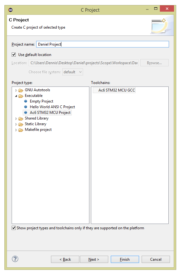
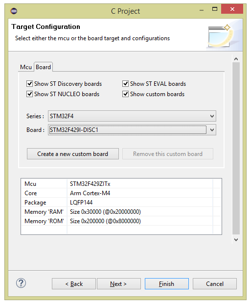
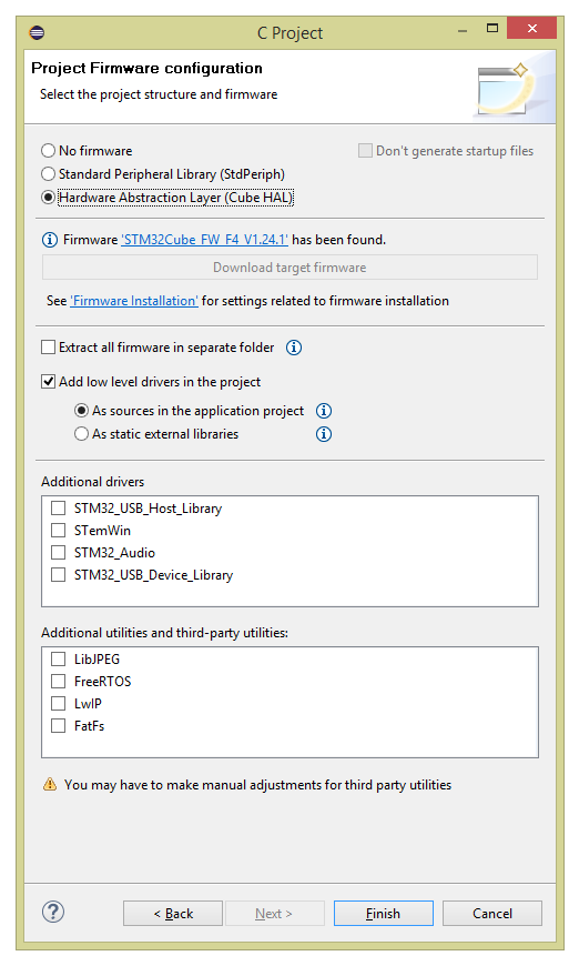
After you’ve got it downloaded and installed, let’s make a new project. Click on File->New->Project and select C Project. If everything installed properly, you should have an option under “Executable” on the left that is Ac6 STM32 MCU Project; select that, give it a name, and hit next and next again on the next screen. When you get to the Target Configuration Screen, select STM32F4 on the Series drop-down and STM32F429I-DISC1 on the Board drop-down and hit Next. Finally, select “Hardware Abstraction Layer (Cube HAL)” in the Project Firmware configuration and hit Finish. This process is detailed in the images below (please click on each of them for the full-sized equivalent).
The Hardware Abstraction Layer libraries are a set of header files that, you guessed it, help you use the hardware built-in to the MCU. The Standard Peripheral Library used to be the de facto standard, and you’ll still see a lot of examples using them out on the web, but they have been deprecated in favor of the HAL libraries, so we will be using those instead.
After completing the above steps, you should have a project folder on the far left screen in Eclipse with the name you typed in. If we open that folder open we’ll see some subfolders of interest:
Binaries – This holds the file(s) that actually get written to the MCU (called an “.elf” file)
Includes – Standard C include files
HAL_Driver – Manuals, include files, and source files for the HAL libraries. We’ll be browsing these a lot.
src – Your own code
inc – Your own include files
Utilities – “Bonus” content, including a folder for the specific eval board we’re using (STM32F429I-Discovery) that has specific header files and source code for how the board is connected (for instance, we can refer to the first LED as LED0 rather than “drive GPIO pin 13 of IO block G”)
Among others
The HAL files are fairly well documented. For instance, here’s a set of comments detailed how to set up the GPIO in stm32f4xx_hal_gpio.c:
/*
                    ##### How to use this driver #####
  ==============================================================================
  [..]
    (#) Enable the GPIO AHB clock using the following function: __HAL_RCC_GPIOx_CLK_ENABLE().

    (#) Configure the GPIO pin(s) using HAL_GPIO_Init().
        (++) Configure the IO mode using "Mode" member from GPIO_InitTypeDef structure
        (++) Activate Pull-up, Pull-down resistor using "Pull" member from GPIO_InitTypeDef
             structure.
        (++) In case of Output or alternate function mode selection: the speed is
             configured through "Speed" member from GPIO_InitTypeDef structure.
        (++) In alternate mode is selection, the alternate function connected to the IO
             is configured through "Alternate" member from GPIO_InitTypeDef structure.
        (++) Analog mode is required when a pin is to be used as ADC channel
             or DAC output.
        (++) In case of external interrupt/event selection the "Mode" member from
             GPIO_InitTypeDef structure select the type (interrupt or event) and
             the corresponding trigger event (rising or falling or both).

    (#) In case of external interrupt/event mode selection, configure NVIC IRQ priority
        mapped to the EXTI line using HAL_NVIC_SetPriority() and enable it using
        HAL_NVIC_EnableIRQ().

    (#) To get the level of a pin configured in input mode use HAL_GPIO_ReadPin().

    (#) To set/reset the level of a pin configured in output mode use
        HAL_GPIO_WritePin()/HAL_GPIO_TogglePin().

    (#) To lock pin configuration until next reset use HAL_GPIO_LockPin().


    (#) During and just after reset, the alternate functions are not
        active and the GPIO pins are configured in input floating mode (except JTAG
        pins).

    (#) The LSE oscillator pins OSC32_IN and OSC32_OUT can be used as general purpose
        (PC14 and PC15, respectively) when the LSE oscillator is off. The LSE has
        priority over the GPIO function.

    (#) The HSE oscillator pins OSC_IN/OSC_OUT can be used as
        general purpose PH0 and PH1, respectively, when the HSE oscillator is off.
        The HSE has priority over the GPIO function.
*/
Let’s blink an LED!
This is basically the “Hello World” equivalent of embedded systems, so let’s get right to it! First off, let’s take a quick peek at the schematic for the board we’re working with. You’ll see on page 6 that we have two LEDs, one green and one red; the green LED is connected to pin 13 of GPIO bank G (that’s on page 5) through a 510 ohm resistor. The red LED is connected to pin 14 of GPIO bank G through a 680 ohm resistor. For this short example, let’s ignore the fancy “Utilities” libraries and use this information from the schematic. So this is what we need in order to create a successful program:
Initialize the system clock (we can technically rely on whatever is the default, but let’s try to start off on the right foot).
Initialize all the HAL stuff and GPIO bank G where the LED is.
Initialize the pin connected to the LED
Drive the LED high and low, with a delay in between of, say, half a second.
Here are the includes we will need:
stm32f4xx.h – General STM32F4 MCU family library
stm32f429.h – LIbrary more specific to the STM32F429 MCU
stm32f4xx_hal_gpio.h – GPIO library
stm32f4xx_hal.h – Another general STM32F4 library, this time specific to HAL
Let’s go ahead and dive into the code for the main function for this quick demo program:
#include "stm32f4xx.h"
#include "stm32f429xx.h"
#include "stm32f4xx_hal_gpio.h"
#include "stm32f4xx_hal.h"

static void SystemClock_Config(void);
void Error_Handler();

int main(void)
{
    // Initialize the hardware abstraction layer libraries
    HAL_Init();

    // Route the clock to GPIO Bank G
    __HAL_RCC_GPIOG_CLK_ENABLE();

    /* Set up the GPIO:
           1. Using pins 13 and 14
           2. Push-pull (rather than open drain)
           3. No pull-down or pull-up
           4. Low frequency (nothing fancy here!)
    */
    GPIO_InitTypeDef g = {GPIO_PIN_13 | GPIO_PIN_14, GPIO_MODE_OUTPUT_PP, GPIO_NOPULL, GPIO_SPEED_FREQ_LOW};
    HAL_GPIO_Init(GPIOG, &g);

    /* Configure the system clock to 180 MHz */
    SystemClock_Config();

    while (1) {
        // Blink the green LED and wait 500ms
        HAL_GPIO_TogglePin(GPIOG, GPIO_PIN_13);
        HAL_Delay(500);
    }
}
As we talked about before, the code above pretty obviously initializes the HAL modules, the GPIO bank we want (bank G), sets up the system clock, and starts blinking the LED. Let’s dig into the GPIO_InitTypeDef structure a little more. The ST Micro libraries follow this module very closely everywhere as far as I can tell – the module is initialized by passing a initialization function a pointer to a structure with all the relavant bits (pun fully intended) you want initialized. In this case, the structure is defined in TODO and reproduced below:
/**
  * @brief GPIO Init structure definition
  */
typedef struct
{
  uint32_t Pin;       /*!< Specifies the GPIO pins to be configured.
                           This parameter can be any value of @ref GPIO_pins_define */

  uint32_t Mode;      /*!< Specifies the operating mode for the selected pins.
                           This parameter can be a value of @ref GPIO_mode_define */

  uint32_t Pull;      /*!< Specifies the Pull-up or Pull-Down activation for the selected pins.
                           This parameter can be a value of @ref GPIO_pull_define */

  uint32_t Speed;     /*!< Specifies the speed for the selected pins.
                           This parameter can be a value of @ref GPIO_speed_define */

  uint32_t Alternate;  /*!< Peripheral to be connected to the selected pins.
                            This parameter can be a value of @ref GPIO_Alternate_function_selection */
}GPIO_InitTypeDef;

// And here's the #defines we can use with the above!

/** @defgroup GPIO_pins_define GPIO pins define
  * @{
  */
#define GPIO_PIN_0                 ((uint16_t)0x0001)  /* Pin 0 selected    */
#define GPIO_PIN_1                 ((uint16_t)0x0002)  /* Pin 1 selected    */
#define GPIO_PIN_2                 ((uint16_t)0x0004)  /* Pin 2 selected    */
#define GPIO_PIN_3                 ((uint16_t)0x0008)  /* Pin 3 selected    */
#define GPIO_PIN_4                 ((uint16_t)0x0010)  /* Pin 4 selected    */
#define GPIO_PIN_5                 ((uint16_t)0x0020)  /* Pin 5 selected    */
#define GPIO_PIN_6                 ((uint16_t)0x0040)  /* Pin 6 selected    */
#define GPIO_PIN_7                 ((uint16_t)0x0080)  /* Pin 7 selected    */
#define GPIO_PIN_8                 ((uint16_t)0x0100)  /* Pin 8 selected    */
#define GPIO_PIN_9                 ((uint16_t)0x0200)  /* Pin 9 selected    */
#define GPIO_PIN_10                ((uint16_t)0x0400)  /* Pin 10 selected   */
#define GPIO_PIN_11                ((uint16_t)0x0800)  /* Pin 11 selected   */
#define GPIO_PIN_12                ((uint16_t)0x1000)  /* Pin 12 selected   */
#define GPIO_PIN_13                ((uint16_t)0x2000)  /* Pin 13 selected   */
#define GPIO_PIN_14                ((uint16_t)0x4000)  /* Pin 14 selected   */
#define GPIO_PIN_15                ((uint16_t)0x8000)  /* Pin 15 selected   */
#define GPIO_PIN_All               ((uint16_t)0xFFFF)  /* All pins selected */
/**
  * @}
  */

/** @defgroup GPIO_mode_define GPIO mode define
  * @brief GPIO Configuration Mode
  *        Elements values convention: 0xX0yz00YZ
  *           - X  : GPIO mode or EXTI Mode
  *           - y  : External IT or Event trigger detection
  *           - z  : IO configuration on External IT or Event
  *           - Y  : Output type (Push Pull or Open Drain)
  *           - Z  : IO Direction mode (Input, Output, Alternate or Analog)
  * @{
  */
#define  GPIO_MODE_INPUT                        0x00000000U   /*!< Input Floating Mode                   */
#define  GPIO_MODE_OUTPUT_PP                    0x00000001U   /*!< Output Push Pull Mode                 */
#define  GPIO_MODE_OUTPUT_OD                    0x00000011U   /*!< Output Open Drain Mode                */
#define  GPIO_MODE_AF_PP                        0x00000002U   /*!< Alternate Function Push Pull Mode     */
#define  GPIO_MODE_AF_OD                        0x00000012U   /*!< Alternate Function Open Drain Mode    */

#define  GPIO_MODE_ANALOG                       0x00000003U   /*!< Analog Mode  */

#define  GPIO_MODE_IT_RISING                    0x10110000U   /*!< External Interrupt Mode with Rising edge trigger detection          */
#define  GPIO_MODE_IT_FALLING                   0x10210000U   /*!< External Interrupt Mode with Falling edge trigger detection         */
#define  GPIO_MODE_IT_RISING_FALLING            0x10310000U   /*!< External Interrupt Mode with Rising/Falling edge trigger detection  */

#define  GPIO_MODE_EVT_RISING                   0x10120000U   /*!< External Event Mode with Rising edge trigger detection               */
#define  GPIO_MODE_EVT_FALLING                  0x10220000U   /*!< External Event Mode with Falling edge trigger detection              */
#define  GPIO_MODE_EVT_RISING_FALLING           0x10320000U   /*!< External Event Mode with Rising/Falling edge trigger detection       */
/**
  * @}
  */
/** @defgroup GPIO_speed_define  GPIO speed define
  * @brief GPIO Output Maximum frequency
  * @{
  */
#define  GPIO_SPEED_FREQ_LOW         0x00000000U  /*!< IO works at 2 MHz, please refer to the product datasheet */
#define  GPIO_SPEED_FREQ_MEDIUM      0x00000001U  /*!< range 12,5 MHz to 50 MHz, please refer to the product datasheet */
#define  GPIO_SPEED_FREQ_HIGH        0x00000002U  /*!< range 25 MHz to 100 MHz, please refer to the product datasheet  */
#define  GPIO_SPEED_FREQ_VERY_HIGH   0x00000003U  /*!< range 50 MHz to 200 MHz, please refer to the product datasheet  */
/**
  * @}
  */

 /** @defgroup GPIO_pull_define GPIO pull define
   * @brief GPIO Pull-Up or Pull-Down Activation
   * @{
   */
#define  GPIO_NOPULL        0x00000000U   /*!< No Pull-up or Pull-down activation  */
#define  GPIO_PULLUP        0x00000001U   /*!< Pull-up activation                  */
#define  GPIO_PULLDOWN      0x00000002U   /*!< Pull-down activation                */
/**
  * @}
  */
The code uses two helper functions, static void SystemClock_Config(void) (sets up the system clock) and void Error_Handler() (acts on errors on initialization of the system clock). Unfortunately, since we can’t do a print or anything like that, all the error handler will do for now is turn on the red LED and hang the program. Here’s the code for this:
/**
  * @brief  System Clock Configuration
  *         The system Clock is configured as follow :
  *            System Clock source            = PLL (HSE)
  *            SYSCLK(Hz)                     = 180000000
  *            HCLK(Hz)                       = 180000000
  *            AHB Prescaler                  = 1
  *            APB1 Prescaler                 = 4
  *            APB2 Prescaler                 = 2
  *            HSE Frequency(Hz)              = 8000000
  *            PLL_M                          = 8
  *            PLL_N                          = 360
  *            PLL_P                          = 2
  *            PLL_Q                          = 7
  *            VDD(V)                         = 3.3
  *            Main regulator output voltage  = Scale1 mode
  *            Flash Latency(WS)              = 5
  * @param  None
  * @retval None
  */
static void SystemClock_Config(void)
{
  RCC_ClkInitTypeDef RCC_ClkInitStruct;
  RCC_OscInitTypeDef RCC_OscInitStruct;

  /* Enable Power Control clock */
  __HAL_RCC_PWR_CLK_ENABLE();

  /* The voltage scaling allows optimizing the power consumption when the device is
     clocked below the maximum system frequency, to update the voltage scaling value
     regarding system frequency refer to product datasheet.  */
  __HAL_PWR_VOLTAGESCALING_CONFIG(PWR_REGULATOR_VOLTAGE_SCALE1);

  /* Enable HSE Oscillator and activate PLL with HSE as source */
  RCC_OscInitStruct.OscillatorType = RCC_OSCILLATORTYPE_HSE;
  RCC_OscInitStruct.HSEState = RCC_HSE_ON;
  RCC_OscInitStruct.PLL.PLLState = RCC_PLL_ON;
  RCC_OscInitStruct.PLL.PLLSource = RCC_PLLSOURCE_HSE;
  RCC_OscInitStruct.PLL.PLLM = 8;
  RCC_OscInitStruct.PLL.PLLN = 360;
  RCC_OscInitStruct.PLL.PLLP = RCC_PLLP_DIV2;
  RCC_OscInitStruct.PLL.PLLQ = 7;
  if(HAL_RCC_OscConfig(&RCC_OscInitStruct) != HAL_OK)
  {
    Error_Handler();
  }

  /* Activate the Over-Drive mode */
  HAL_PWREx_EnableOverDrive();

  /* Select PLL as system clock source and configure the HCLK, PCLK1 and PCLK2
     clocks dividers */
  RCC_ClkInitStruct.ClockType = (RCC_CLOCKTYPE_SYSCLK | RCC_CLOCKTYPE_HCLK | RCC_CLOCKTYPE_PCLK1 | RCC_CLOCKTYPE_PCLK2);
  RCC_ClkInitStruct.SYSCLKSource = RCC_SYSCLKSOURCE_PLLCLK;
  RCC_ClkInitStruct.AHBCLKDivider = RCC_SYSCLK_DIV1;
  RCC_ClkInitStruct.APB1CLKDivider = RCC_HCLK_DIV4;
  RCC_ClkInitStruct.APB2CLKDivider = RCC_HCLK_DIV2;
  if(HAL_RCC_ClockConfig(&RCC_ClkInitStruct, FLASH_LATENCY_5) != HAL_OK)
  {
    Error_Handler();
  }
}

void Error_Handler() {
    // Oops. Bad stuff happened! Let's turn on the red LED.
    HAL_GPIO_WritePin(GPIOG, GPIO_PIN_13, GPIO_PIN_SET);

    while (1) { }
}
Don’t worry too much about SystemClock_Config(void) yet – it’s a copy-pasted version of ST’s standard clock configuration function for running the system at 180 MHz. We obviously don’t need to run the processor at it’s maximum clock for blinking an LED, but we’ll likely end up running it at this frequency in the finished product. We will dive more deeply into how that code gets generated inside the STM32F4CubeMX software in a few posts.
That’s it for this post! After you put the code above in one file (main.c) and build (using the hammer icon), you can program the board by right clicking on the project (the folder) and selecting Target -> Program Chip. You can tell the IDE to reset the board and you should see the green LED start blinking right away like in the below animation!
See you next time for some fun running the demos ST Micro includes with their libraries on this evaluation board and another short example!.
Picking out a microcontroller is a bit of an arcane art; the requirements are often hazy, the process is full of pitfalls, everyone’s got a different opinion, and it usually feels like the only way to succeed is to have done it before and gotten it to work. This is so much the case that people tend to stick with whatever manufacturer/part family they’ve worked with before – check out the (often very fervent) discussions between the two biggest camps for hobbyists, the Atmel AVR group (if you’ve heard of Arduino, this is a superset of that) and the Microchip PIC group, and that’s now the same manufacturer (Microchip acquired Atmel in 2016)!
I’ve picked out a processor already (yes, you guessed it, it’s something I’ve used before), but let’s walk through some of the considerations here, both for this project in particular as well as any project in general. But first – what is a microcontroller? What’s a microprocessor? What’s the difference?
The “micro” in microprocessor just means small and, as far as I know, it’s an arbitrary designation on some processors and controllers. In fact, while I’ve heard of “just processors” (no micro) like the many parts Intel makes for desktops and laptops, I’ve yet to hear of “just controllers.” From a very high-level point of view, a processor (micro or not) is a chip that will run code – it has several “subblocks” inside of it that help it do it, like a small amount of memory (L1/L2 cache, registers), the Arithmetic Logic Unit (ALU – how the processor “does math”), hook-ups for external memory and other interfaces, and many other things that I’ve since forgotten. A microcontroller is a chip that has a microprocessor inside of it as well as other internal blocks, the nature of which depend on the specific controller (some examples: ADCs, DACs, more internal memory, LCD display controller, analog comparators, …). Having these blocks to hook up to can be quite handy, as we’ll see in our project.
High-Level Considerations
Here’s a list of some common microcontroller specifications to get us started:
“Speed” – How “quickly” the internal microprocessor runs – typically measured in instructions per second (or more coarsely by the CPU clock)
Internal memory – How much ROM and RAM the microcontroller has internally in its caches as well as for general use – if it has enough of it, we might get away with not having an external memory chip
“Modules”/interfaces – Internal ‘components’ the microcontroller has, like ADCs, DACs, etc. or interface hook-ups like supporting Ethernet or USB
Architecture – This is a high-level way of describing how the microcontroller is “organized” inside (in terms of how things are connected internally and how time intensive it is to perform certain tasks, like reading a byte from memory). I include “how many bits” are in the processor in here as well, for example, a 32 bit ARM processor vs a 16 bit MIPS processor. This also determines the maximum amount of memory the microcontroller can interface with.
Power usage – How much power the chip consumes (this is usually specified under “normal load”, in some sort of “sleep” or “suspended” mode, and under “maximum load”). This is a very important spec. for battery-powered products that want to last as long as possible before needing to be recharged.
Footprint – What the chip pinout looks like physically – this affects the layout as well as the solderability (assuming we’re putting the board together ourselves)
“Tools” – This list is very important (perhaps the most important consideration if we’re working on a project by ourselves)
Programmer – Do we need to buy a programmer that connects to a computer to “write” the code to the chip? How easy is it do so?
Utilities – Does the manufacturer provide header files and basic functions for each of the microcontroller “modules” or do we need to write everything ourselves from the datasheet?
Evaluation board – Does the manufacturer provide a design (schematic and layout files as well as a board you can sample or buy) that they’ve “blessed” as being good? It can be incredibly useful to have a model to emulate.
Websites – Is this chip often used by other hobbyists? Can we find helpful websites with examples and/or forums where we can ask questions if we get stuck with something? This is a very important consideration, especially if we’re planning on doing this project alone (that is, without the help of a friend that’s done this or something very similar with the same microcontroller).
Let’s think about what requirements we need for this project in particular, in the same order as above (if you haven’t read part 1 of the series, consider giving it a quick glance before continuing):
Speed – There’s nothing from the design point of view that requires the microcontroller to be extraordinarily “fast” if we implemented the sampling hardware as we discussed in part 1 of the series. That said, we’d still like to processes those samples quickly once we’ve gotten a trigger and send them off to the display to create a “responsive system”, and that’ll require some quick thinking. If our maximum sampling frequency is 50-60 MHz, let’s try to pick something at or above 100 Megainstructions Per Second (MIPS) to keep up with this. This is very much a number that I pulled out of nowhere (there’s nothing magical about “2 instructions per sample”), but consider that we don’t need to optimize for power consumption or anything else that would increase with the speed of our processor (other than cost), since this will just be a bench-top oscilloscope; so let’s see if we can find an affordable 100 MSPS chip to use.
Here’s a list of helpful modules:
TFT display controller – An internal module that generates the right clock signals for driving the LCD-TFT displays that are common in embedded systems. This is highly preferable to a much slower SPI-based (Serial Peripheral Interface, a very common interface in almost all controllers) display that we’d be forced to use without the built-in display controller.
Internal ADC – We’re not going to find very many internal ADCs that can sample at 50+ MSPS (yes, amazingly, some exceptions do exist). Even if the internal ADC is fast and everything we could ever want, we’re not going to find a microcontroller with an “oscilloscope triggering logic block” like what we discussed on part 1. However, an internal ADC (even if it is slow) will be useful for debugging and writing the code while we’re still working on our external sampling hardware. As I alluded to in the project page, we can also use the development board’s internal ADC to debug our oscilloscope design.
Internal DAC – It’d be nice to generate some analog signals on the development board that we can then look at with our scope to test it (for those of us who don’t own function generators).
Internal memory – This is more of a “wishlist” item, but ideally we have enough memory that we don’t need any external chips (except for the signal samples as we discussed in part 1 and the display memory)
Plenty (say, about 40) of IOs that we can break out into header pins for when we make mistakes
At least one of each SPI and I2C interface because we’re likely going to need them for something (even if it’s just for an on-board temperature sensor)
Architecture – I don’t think we have to be picky on this one. I’ve used (and liked) ARM processors in the past, but I’m happy to try something new, too. And we don’t have to worry about interfacing with large amounts of memory, either.
Power usage – We’re not running this off a coin cell battery, so we’re again not super picky; but it’d be nice if it didn’t heat up like bonkers. Let’s try to keep it at or below a Watt.
Footprint – Something we can solder without the use of a reflow oven or heat gun – this disqualifies all BGA or QFN packages, for example.
Tools
Programmer – I want to be able to program this from a computer’s USB port (please no RS-232 port requirement). If I have to buy a programmer, I’d like to spend less than $50 on it.
Utilities – I’ve started a project before with just a datasheet and written the assembly code to interface with all the registers. I’d rather not do that directly again, and I don’t think that would be the most instructive use of our time (maybe on another, smaller project). I want good header files and cross-platform support for writing and compiling the code. I’m OK with using a “manufacturer sanctioned” IDE to write the code so long as:
I don’t have to pay for using the IDE
The fact that I’m not paying for the IDE doesn’t restrict me (for example: can only compile projects <32KB in size; yes, I’m looking at you, Keil)
Yes, I want an evaluation board, and I plan to use it heavily for developing the initial code as well as debugging my own board.
Some amount of support would be nice for this project, but I think not crucial. It’s one of the only things on this list I’d be flexible compromising on.
So what are we going with?
I decided to use ST Micro’s STM32F429 (datasheet) microcontroller. I like the STM32F4 series quite a bit; I used several of these on a project at college where a group of us tried (and failed) to build an electric car. The MCU worked well, though! Here’s what it has going for it, in the same order as above:
180MHz max CPU clock, 225 MIPS. We can get a lot done with this chip!
Helpful modules:
1 or 2MB (depending on the exact model) of integrated Flash memory for storing code. Way more than what we need.
256KB internal RAM – probably sufficient. How many variables do we need, anyway?
LCD TFT controller and parallel interface (this only comes with the STM32F429 version – the STM32F407 and STM32F427 MCUs are more general chips without the LCD stuff)
3 12-bit, 2.4 MSPS ADCs – not bad at all for a debug tool; we can make two channel scope to debug our real scope.
2 12-bit DACs – excellent
A bunch of IOs (how many exactly depends on which model you get, but at least 40 of them, given the smallest package is 100 pins)
SPI and I2C
32-bit ARM processor and a good DMA controller to interface to external memory if we need it (we will at least need some SDRAM to store the data for the LCD pixels)
At 270mA max current draw, the total maximum power consumption is 3.3V * 0.27m = 0.9W, right about our target. But I don’t think we will hit this maximum number, as we won’t always be working the processor to its fullest.
The BGA packages are a no-go, but the LQFP packages are OK to hand-solder
Tools
The ST-Link programmer is just $20, but even better, the eval board comes with that functionality out of the box (you program it through a simple micro USB connector). And according to people online, we can rewire the eval board to program our own custom board! That’s great news.
ST provides extensive header files and examples for this family. For every module (e.g. for the display on the eval board), ST provides example code for interacting with it in one big package called STM32CubeF4. There is a free, open-source IDE called SW4STM32 built on top of Eclipse we can use on Windows or Linux for compiling, linking, and locating the code, and we can program the chip directly from there.
The eval board for this MCU is called 32F429-Discovery and it comes with a display and everything! To give you an idea of how relevant this board is our project, check out this video of a homemade scope project running on the eval board itself!
This family of processors has a decent following online. As an example, check out STM32F4-discovery. At the very least we will probably be able to get answers to our basic questions.
Curious for more?
Sorry for throwing a bunch of specs and text at your face. In the next few posts you’ll be able to see the microcontroller in action (I’ll walk you through how I set up my computer to program it and quite a few examples with it) and hopefully that’ll justify the choice far better than the wall of text above. It should also be a little more exciting.
An oscilloscope (or just “scope” if you’re far enough removed from microscopes for it to not be confusing) is a tool that measures and reports voltage over time (a “signal”). Modern oscilloscopes are digital and will show the signal (or various signals at the same time) on a LCD screen. There’s a host of buttons that control which part of the signal is shown and when (and/or how often) the signaled should be “sampled.” It’s a very useful tool that lets you verify that the signals on your board are actually doing what they’re supposed to do, without degrading too much in the process.
Let’s get into it below.
So – what makes a scope good?
It should go without saying an oscilloscope should be accurate and should introduce as little noise as possible. You want to make sure that what you’re seeing on the screen is what is actually going on where you’re probing. This is a simple concept to understand, but it’s easier said than done.
An oscilloscope should also be as generic as possible – ideally, you want an oscilloscope that is a “one size fits all solution”; you don’t want to reach for different oscilloscopes when working on different parts of your project. What this means practically is that you want to be able to “zoom in and out” of the signal in both the vertical and horizontal axis (as well as shift it up and down and left and right). This will make your oscilloscope be able to display the widest variety of signals – small or large (y-axis), fast or slow (x-axis). It will also allow the oscilloscope to look at a single signal in various ways (zoomed-out on the x-axis for long-term, steady state behavior or zoomed-in on the x-axis for short-term “transient” behavior, such as spikes or noise, for example).
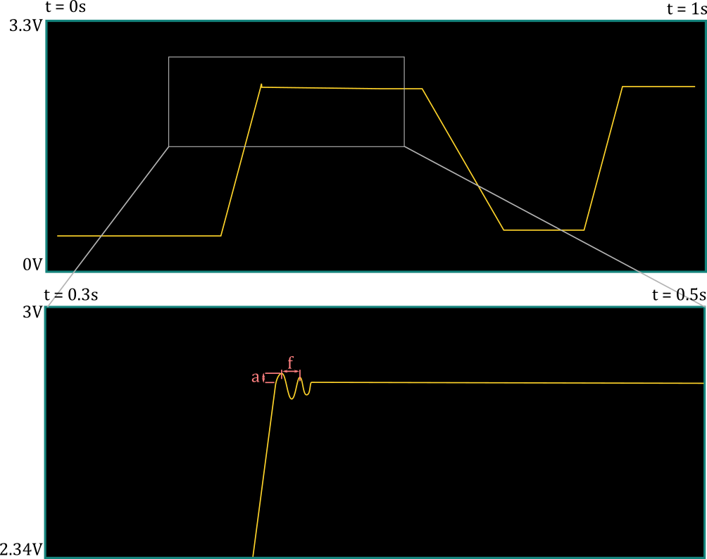
The vertical axis represent voltage, so to “zoom in” you need to amplify (increase the amplitude of) the signal and to “zoom out” you need to attenuate (decrease the amplitude of) the signal. This is done in what we call the “analog front-end” of the signal. The horizontal axis represents time, so to “zoom in” we’ll need to take samples more frequently and to “zoom out” we’ll add more time between the samples. Here’s a quick example:
Example of zooming in to a signal on an oscillocope
What is actually happening when we zoom in like in the above example? We can say that we adjust the “screen” so that it goes from showing what it was previously to being filled by only what’s in the grey box. That is, the screen is now limited to showing a “subset” of what it showed before – instead of voltage going from 0V (bottom of the screen) to 3.3V (top of the screen). now it only goes from 2.34V to 3V. Likewise, the time scale has been reduced – now it only goes from 0.3s on the far left of the screen to 0.5s on the far right of the screen. This sounds a lot like a “digital zoom” on a camera, but if we take a closer look at the second image, we see that we didn’t simply reduce the amount of information – we now have more information about the little “spike” we saw in the zoomed-out version. What before looked like a simple “spike” now looks like oscillatory behavior with an overshoot of a and a frequency of f.
To understand what’s going on, we have to know what’s going on in the guts of the scope to show you this signal on the display. Here’s a simplified block diagram of the hardware that obtains the signal to be displayed (we’ll expand on this later):
The microcontroller (MCU) is the brains of the operation – it runs the code that we write and tells the display what pixel goes where (and in what color). A microcontroller by itself, however, does not understand an analog signal; it works purely in the digital domain – ones and zeroes, or 3.3V (or other IO voltage) and GND. The MCU also doesn’t have a sense of “analog time” – it’s fed a clock from a crystal oscillator or other source, and runs an instruction (think of a line of code) every tick (this is again an oversimplification, but it’s a good enough description for our purposes).
The MCU needs a series of digital signals that somehow map to the original analog signal. This is the job of the ADC (Analog to Digital Converter), which takes in an analog signal at the input as well as a digital clock and spits out the “digital equivalent” of that signal at the output whenever the clock goes from low to high (or sometimes high to low). The voltage range at the input of the ADC, however, is limited within a certain range, typically (but not always) between ground and the ADC’s supply (3.3V or 5V, for example).
This is why we have an analog front end – it needs to process the analog signal so that it fits within the dynamic range of the ADC (the min and max voltages at the input that it can understand). It’ll need to make the signal bigger or smaller (scale the amplitude of the signal linearly) as well as shift it up and down so that the user’s desired range/window is within the ADC’s dynamic range. This amplitude factor (gain) and offset will need to come from the MCU so that the user can configure how the signal is seen on the screen.
We need something else between the MCU and the ADC. The ADC will be sampling the signals constantly; in order to support a wider range of “zooming” on the signal, we will sometimes need to sample the signal very often, if the user wants to zoom way in on the signal. For instance, if the user wants to the screen’s width to be 1us, the screen is 300 pixels wide, and we want each pixel to represent a sample, we’ll need to take a sample every 1us / (300 px/sample) = 3.33ns, which is a sampling frequency of 1/3.33ns or 300MHz (that’s very fast)! Realistically, we wouldn’t do a sample per pixel – we can start with a sample every ten pixels and connect them with a line – but you get the point. We’ll see that the ADC cost starts to increase astronomically with the maximum sampling frequency, so that will be the limiting factor here – probably somewhere around 50-60 MHz; I’ll show you the options and we’ll do the analysis together. In any case, the MCU cannot handle 50 million samples a second. Let’s say a typical embedded processor runs at a clock frequency of 200MHz – that’s 4 cycles per sample if we’re sampling at 50MHz – there’s no way it’ll be able to do the triggering, processing, displaying instructions, and anything else it needs to do in those four cycles of “free time” before the next sample comes in!
What we need to think about here is that, in practice, most samples a scope takes are thrown away and never displayed. That makes sense – there’s no way a human brain would be able to processes 50 million (distinct) samples a second (although you would get some benefit from displaying 1000 samples that were an average of 50 million – but let’s put that aside for now). The scope setting that determines which samples are thrown away and which are shown on the screen is called the trigger. Triggering circuitry can be arbitrarily complex, but at its simplest the user configures what threshold voltage they’d like to see, and whether they’d like to see the signal cross that voltage from below (rising edge), above (falling edge), or both. The scope then displays samples around that triggering voltage – typically some samples that happened before it and some that happened after (the exact delay between the trigger and the samples shown on the screen can also be configured by the user). The trigger can also be set to “auto” – which means the scope will “continuously” show samples – but realistically, this doesn’t mean you see all the samples. In fact, what most scopes are doing is waiting for a trigger event to happen, and if they don’t see one, then they will trigger themselves after a preset “timeout”, which makes it look like the scope is running continuously.
What this means in practice is that the MCU doesn’t need to look at every sample from the ADC – what we should try to have instead is some hardware that looks at every sample and figures out if a trigger event has happened. This same hardware can be responsible for saving the samples to memory (remember – both before and after the trigger, so we need to be continuously storing the samples, not just after we see a trigger) and managing the memory so we don’t overflow it with samples that we’re never going to need. Once the trigger has happened, our circuitry can let the MCU know that it needs to get the samples and can tell it where exactly in the memory to look for the samples. The MCU can then take its time, read the samples out of memory, and display them.
Here’s what we need, then, to make an oscilloscope that is as generic as possible – each of these will warrant several posts of their own:
An analog front end with a variety of MCU-controllable settings to both scale the signal as well as offset it
An ADC capable of sampling the signal as fast as possible without breaking the bank
A flexible and MCU-controllable triggering and logic circuit to process and store the “interesting” samples coming out of the ADC.
A good amount of memory for the samples, so that we can support a delayed version of the signal (make the signal move left or right on the scope screen)
A decently fast MCU and a good display to make sense of the samples
Don’t worry if there are parts of the above concepts that seem too complicated to grasp now – we’ll delve into each of these elements in more detail individually (and if you’re angry that I got a lot of stuff wrong or oversimplified, I hear you – I’ll be learning more throughout this process too). What I’m hoping you’ll get from this, however, is that hardware design is often fitting blocks together to get what you want. You start with what you know (“I need an MCU”), figure out what it can’t do (analog signals), find a component that can (an ADC), and iterate from there (“the ADC’s input dynamic range is limited”). This is one of my favorite aspects of hardware design, and I hope it intrigues you, too!
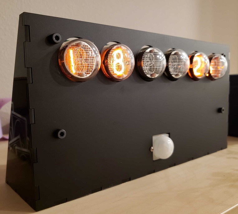
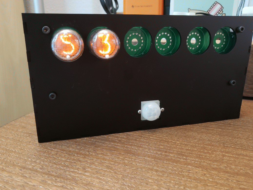
We did it, folks! It’s at least functional, which is more than I can say for a lot of my own personal projects that I’ve started! I’ll even dare to say that I think this even looks better than the inspirational picture I posted on my first post!
The clock from an odd angle
The full enclosure, with the tubes recessed a little bit more using 20mm standoffs
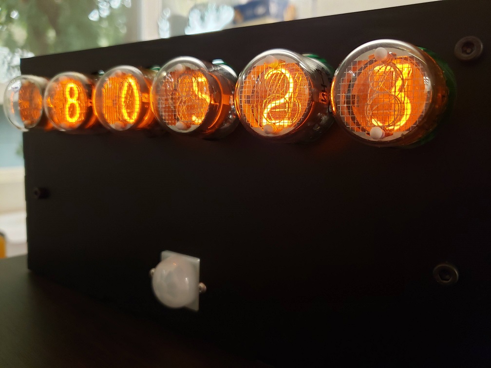
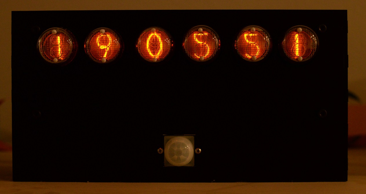
Finished clock showing the time (dark image so you can better see the glow of the tubes)
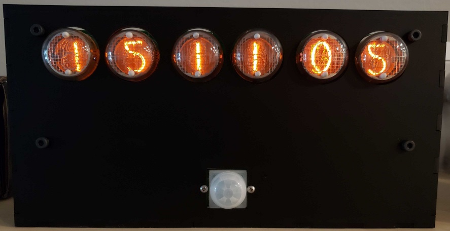
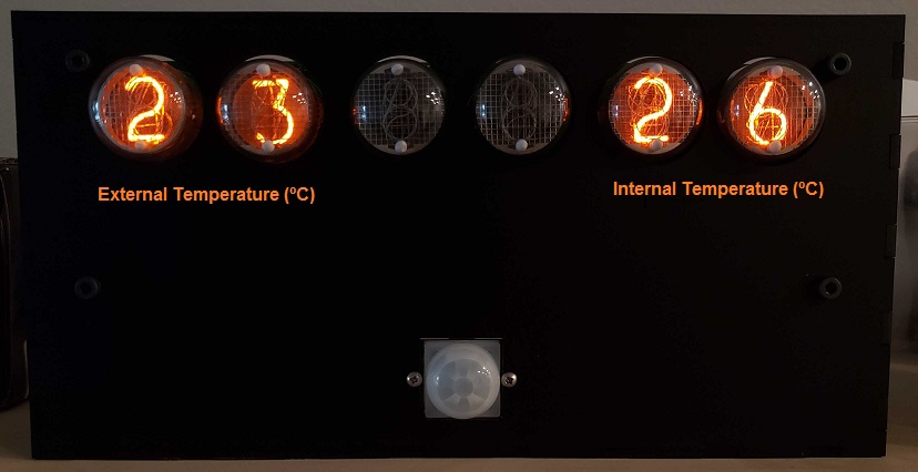
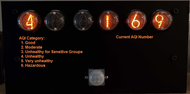
The clock shows the time, the internal temperature, the external temperature (based on querying OpenWeatherMap API with the right city code), and the AQI (air quality index using the AirNow API – a good idea for us in the west coast of the US who happen to be experiencing a lot of smoke in the air!). Right now I’ve got it alternating between the time, the internal and external temperatures (in one screen), and the AQI. The temperature units can be set to Celsius or Fahrenheit. Right now I cycle between these three “screens” every 20 seconds.
Time (HHMMSS)
Temperatures
AQI (there was smoke this day!)
The PIR sensor is working well, too! I tuned the time it would have to go without seeing motion to fall asleep to a minute; this seems to work well because it’s enough time to cycle through all three screens and because I put the clock in a rather central location where it’s easy to wake it up by waving at it. The sensor has a 7m range in a 120 degree cone, which turns out to be just about perfect. I was having issues making it work initially and then I realized that I was giving it a 3.3V supply when it wanted to be connected to 5V – oops! In my defense, it specs 3-5V on the Adafruit website, but then there’s a little bit of text saying that if you want lower voltages to work you have to bypass the regulator on the PIR sensor board which I completely missed. It was easier to connect it directly to 5V instead, so I went ahead and changed the wiring to make that work. I’ll clean up the code a little bit more, edit my code post from last week, and post it there.
The project is more or less “done” now, but I’ll do a couple more review posts where we’ll look at reducing the cost of the whole product as well as making it easier to put together. Specifically, I’d like to:
Improve the nixie footprints by rotating them clockwise slightly and make all of the holes significantly larger; this should allow the person soldering the tubes to rotate them in position and then solder them.
Move the power supply onto the main board
Remove the 40pin ribbon cable and allow a RPi Zero W to be directly connected instead (via a 90 degree header). Margaret has one that I can try to make sure it works OK (I can’t think of why it wouldn’t)
Clean up and fix a few things on the PCB
Try out multiplexing the tubes; if this looks good, I’ll do so on the final clock to reduce the number of necessary IOs. That will allow me to add a SPI/I2C temperature sensor to put on the board for a better sense of the room temperature.
I’ll also keep you updated on any new feature changes or other things I try, of course. One thing I’m thinking of doing is buying a Bluetooth temperature and humidity sensor like this one (you can bet that’s not an affiliate link!) and connecting it to the clock.
I haven’t posted in a little while – I’ve been putting off soldering down the nixie tubes onto the board (mostly because it’s a little annoying to bend the pins so that the tubes are vertical), so I’ve been working on writing the code for the project. I’m periodically interspersing the tube soldering, so I’ve only got two left! Anyway, I realize nobody wants to just see a bunch of code on a blog post, so bear with me as I try to make the information a little more digestible while preserving the important bits of this part of the project.
Language
The Raspberry Pi will run basically anything you’d like on it as it’s just a Linux box. I decided to code this up in Python for simplicity and because I’ve done plenty of GPIO toggling in it before. However, you may notice that the design is very procedural, as if it were written in C – I guess my mind went to that immediately when I thought of doing an embedded systems project; now that I think about it, it may be more prudent to design the code in a more object-oriented kind of way – by, for instance, creating instances of objects for each nixie tube that hold member variables for their IO lists and states as well as member functions for writing a digit and so forth. I may overhaul the code, but this works for now.
Initialization
I designed the code such that there would be no global variables, although I do have “constants” (Python can’t enforce that they stay constant) that are global. Here’s the constants, divided by category:
Name
Value
Description
SLEEP_TIME
30
Number of ms to sleep between every cycle of the main loop
CYCLES_PER_SECOND
1000 / SLEEP_TIME
Number of code loops (cycles) per second
SECONDS_PER_MINUTE
60
The number of seconds there are in a minute (now that’s a constant!)
EXT_TEMP_UPDATE_SECONDS
15 * SECONDS_PER_MINUTE
How often (in s) to update the external temperature (the API call is a little slow)
INT_TEMP_UPDATE_SECONDS
SECONDS_PER_MINUTE
How often (in s) to update the internal temperature
Constants for keep track of time
Name
Value
Description
BUTTON_IO
10
IO pin on the Raspberry Pi header to which the button is connected
PIR_IO
8
IO pin on the Raspberry Pi header to which the PIR sensor is connected
BUTTON_PRESS_INIT_VAL
CYCLES_PER_SECOND / 15
How long the button needs to be held down for to register a press – for deboucing (2 cycles)
BUTTON_HOLD_INIT_VAL
CYCLES_PER_SECOND * 3
How long the button needs to be held down to register a hold (3 seconds)
PIR_DETECT_INIT_VAL
1 * CYCLES_PER_SECOND * SECONDS_PER_MINUTE
How long the PIR detector has to go without detecting motion before putting the Nixie tube display to sleep (1 minute)
Constants for IO interfaces
In addition to the above constants, there’s also a few constants required for the API calls (the strings and API keys) in the file nixie_helpers.py, as well the constant ROOM_TEMP_OFFSET, which is the temperature offset in Fahrenheit between the CPU temperature and the room temperature. I calibrated this out with a thermometer and it’s around 34°F at my place.
The sole initialization function is initGPIOs(), which builds and returns a list of lists, where each one of the lists corresponds to the IO pins connected to the four bits driving the nixie tube decoders of that digit. So, for instance, the numbers in dig_H1 = [11, 7, 5, 3] correspond to the four IOs connected to the four binary bits on the decoder driving the tube of the first hour digit. This (and the rest of the connectivity) is illustrated below.
The function then initializes these GPIOs, configures them as outputs, and initializes the input GPIOs corresponding to the button and PIR sensor. The list of nixie tube IOs is returned to the Main() function to be used later for displaying the digits.
Variables
The variables are all initialized and kept track of locally in the Main() function. Here’s the table of these variables:
Name
Value at Initialization
Description
button_press_timer
BUTTON_PRESS_INIT_VAL
How long the button must be held down for checkButton() to register a button press (this is done with the timer reaches zero)
button_hold_timer
BUTTON_HOLD_INIT_VAL
How long the button must be held down for checkButton() to register a button hold (puts the clock display to sleep or wakes it)
pir_timer
PIR_DETECT_INIT_VAL
How long the PIR sensor must go without detecting motion to put the clock to sleep (also done when the timer reaches zero)
current_mode
Mode.TIME
This is set to an IntEnum type that tracks the current mode – TIME, INT_TEMP (CPU temp), or ALTERNATE. I’m planning on adding an EXT_TEMP to get the external temperature later.
is_asleep
False
Whether the clock is asleep (True) or not (False)
IO_list
return value of initGPIOs()
The IO list of all the Raspberry Pi IOs connected to the decoders driving the Nixie tubes
temp
Current external temperature
The external temperature. This variable gets updated every EXT_TEMP_UPDATE_SECONDS
aqi_cat
Current AQI category
The current AQI (Air Quality Index) category, from good to hazardous. This variable also updates every EXT_TEMP_UPDATE_SECONDS
aqi_num
Current AQI number
The current AQI number, from 0 to 500. This variable also updates every EXT_TEMP_UPDATE_SECONDS
last_weather_time
Now
The last time the external weather was updated
int_temp
Current room temperature
The current room temperature
last_int_temp_time
Now
The last time the room temperature was updated
Local variables for this project
Helper Functions
There’s a few short functions in the file aptly named nixie_helpers.py. They’re pretty self-explanatory, so I’ll just summarize them in a table:
Name
Argument
Description
kelvinToC
temp (in K)
Returns the Celsius equivalent of temp
celsiusToF
temp (in °C)
Returns the Fahrenheit equivalent of temp
fahrenheitToC
temp (in °F)
Returns the Celsius equivalent of temp
getTemperatureAPI
unit (Temp_Units)
Returns the temperature from the OpenWeatherMap API in the unit corresponding to unit
getAQIAPI
N/A
Returns the AQI category and number from the AirNow API
getCPUTemp
unit
Gets the CPU temperature in the unit corresponding to unit
getRoomTemp
unit
Gets the room temperature (CPU temperature with an offset) in the unit corresponding to unit
Software Loop Design
I designed this as a polling based system that checks on the status of the IO inputs (the button and the PIR), updates its internal variables with the current time, weather, and CPU temperature, and writes to the IO outputs (the decoders driving the Nixie tube) every so often (so that there are CYCLES_PER_SECOND number of cycles per second). After it has completed its tasks, the loop sleeps for SLEEP_TIME (in milliseconds) and starts again from the beginning.
This is the piece of code that the Raspberry Pi continuously runs every cycle. The first function that is called is the checkButton() function. This function takes in the current values of the timers for pressing and holding the button, and decrements them if the button is pushed; otherwise, the timers are reset if the button is not pushed. The function returns the new timer values as well as booleans for whether the button was pushed or held. The function does not register continuous button presses – that is, the button must be released in between two button presses for it to count as two presses instead of one long button press.
Next, checkPIR() is called. This works in a similar way to the above – it takes in the pir_timer and decrements it if is not detecting motion this cycle; otherwise, it resets it. The function returns the new timer as well as a boolean indicating whether no motion has been detected for the full PIR_DETECT_INIT_VAL time.
After this, getDisplayString() is called – this function takes in current_mode, is_asleep, and a value (time, temperature tuple, or AQI tuple) and uses these parameters to determine what to display on the nixie tubes – whether that’s the time, the temperatures, the AQI, or turning the display off. This function returns a string in the form “DDDDDD”, where every “D” is a digit from 0 to 9, or the character “A” if that particular digit is meant to be turned off.
Finally, updateDisplay() is called with IO_list and the string returned from getDisplayString() as arguments and displays the correct string on the nixie tubes or throws an exception if it gets a malformed string as an input.
After all this, the loop repeats and again begins by polling the inputs.
Full Code
Please also note that, since I forgot to order a push-button, I haven’t tried that part of the code yet! You can find the repository (hardware design and code) on the main project page. Or you can browse the two files directly on the repository by clicking the following links: main.py and nixie_helpers.py.
The first enclosure I’ve ever designed arrived a few days ago (I wonder if it still count as an enclosure if it has an open back, as it’s not fully enclosing anything)!
I did a quick fit test with the board and some standoffs and it looks pretty good. I’m so happy that my cut-outs for the tubes and the PIR sensor worked out well!
Front view
Back view
I’m very impressed with the material and with the laser cutting service. Everything fit well (if I were to remake this, I would probably shave a quarter mm from the joints as they were a little tricky to put together, but that’s on me) and I’m very happy with how it looks. Here’s some more detail on the material, which has a matte (external) and glossy (internal) side. I chose to put the matte side on the exterior because I don’t want my fingerprints all over the face of the clock, but there’s one face (the triangular face on the left) that’s inverted due to the orientation it was in when it was cut – something to thing about for next time.
Matte side
Glossy side
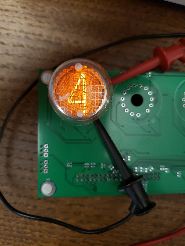
I also wrote a quick script to display the seconds portion of the current time on the two tubes I’ve got soldered down, and that”s worked well except for some digits missing due to some questionable solder joints.
Displaying the current seconds rather than the hours
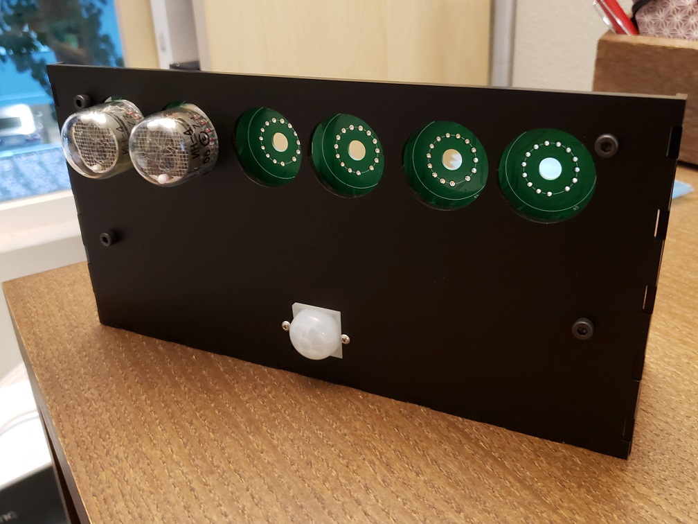
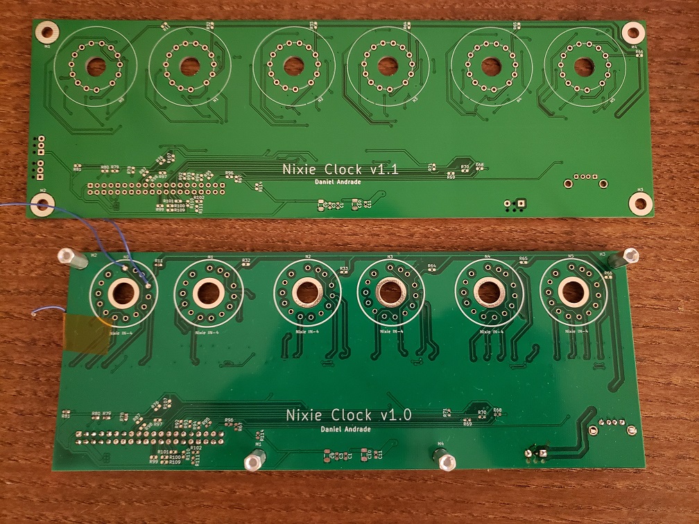
The new boards arrived early this week! Here’s a side by side comparison of the old board and the new one (notice the difference in the of the white silkscreen around the tubes – the new silkscreen reflects the actual size of the tube, whereas before I think I just plotted down a circle of arbitrary radius).
Board comparison. I’m not super jazzed about the new green soldermask color, but otherwise the new board is all right.
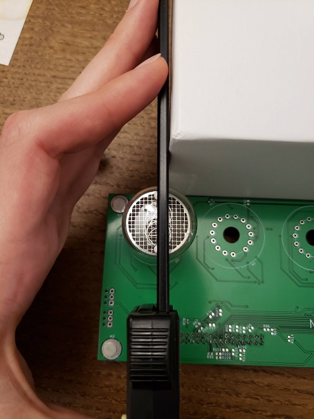
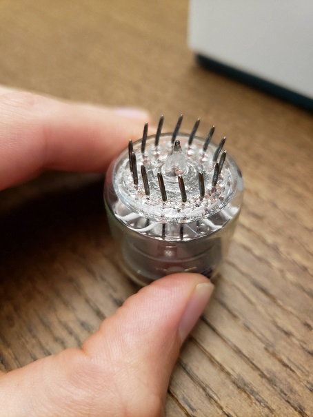
I finally bit the bullet yesterday and installed one of the tubes on the new board (after installing the decoder and series resistors and testing that out). It was a bit of a process because it turns out that the alignment of the tube itself to the pins is not completely controlled. So when I put all six of the tubes down on the board (with no solder), they were all at slightly different angles!
I may have to come up with a way to combat this if I want to make clocks for everyone in my family, but for now, I settled with bending the pins and aligning it manually. My girlfriend gave me the idea to align the two white dots using a box and my calipers as right angles, as seen below.
Aligning the Nixie tube using the two dots and two straight-edges
The pins turned out pretty wacky, right?
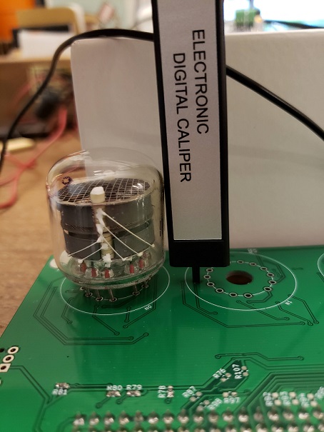
Making sure the height of the tube is even all the way around
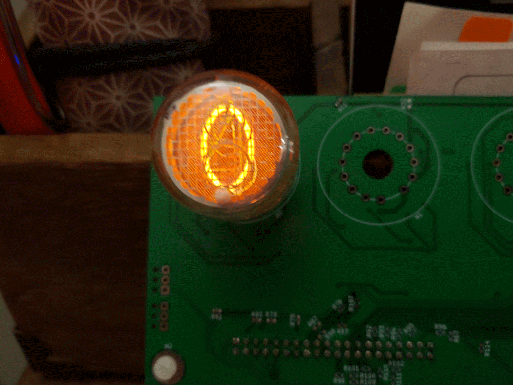
After this I tested each digit manually (by driving each pin with the supply and a series 15kΩ resistor), soldered it down, hooked it all up, and wrote a little program to count up (and then go back to zero). I made a little animation to show you!
Testing each digit before fully committing and soldering the tube down
It works!!
Now there’s no excuse. It’s time to get everything else soldered down while I wait for the enclosure to arrive!
It’s a new post in the series and this time there isn’t a new PCB! So there is hope after all…
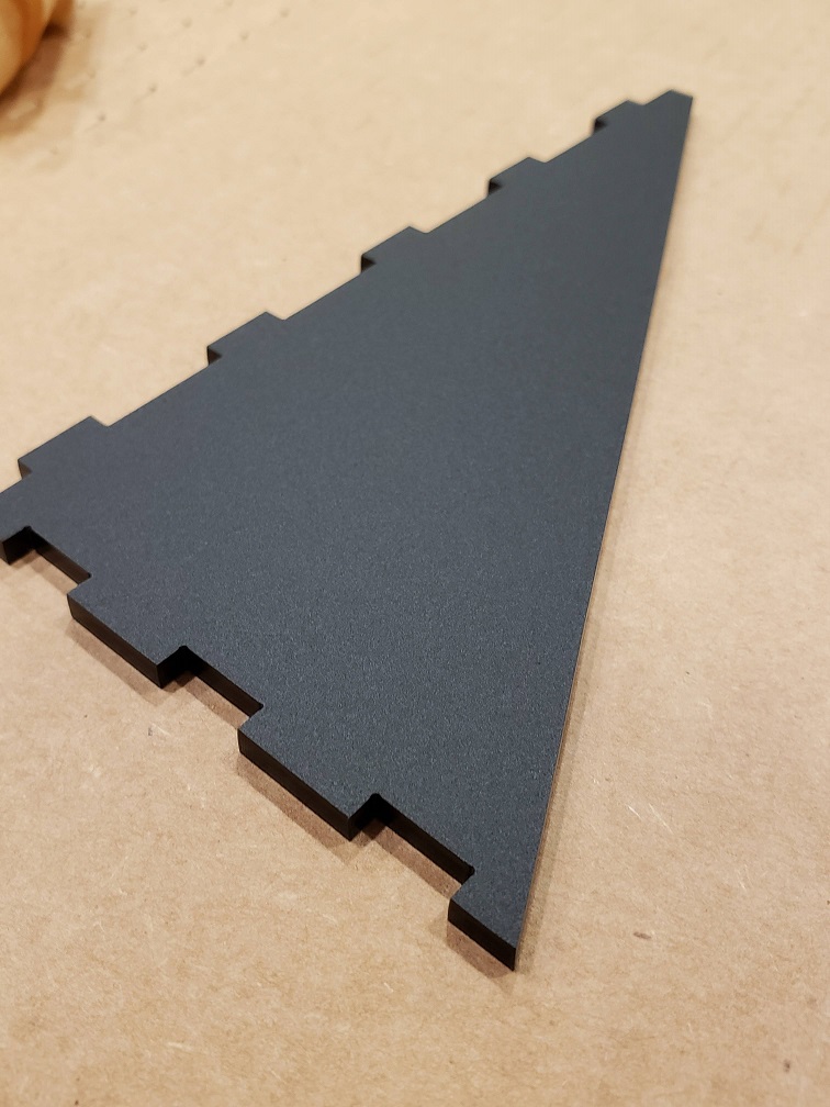
I haven’t had much of a change to work on the electronics part of the project since the new board hasn’t arrived yet, so I’ve been mainly focusing on the enclosure design aspect. A friend of mine suggested looking more into manufacturing techniques before continuing, so I took his advice and decided I’d give laser cutting a go for my first prototype. I really like how the finished products look with this technique and it seemed cost effective for a larger design like this one.
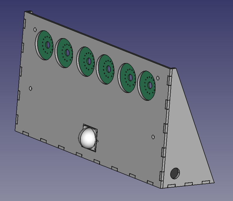
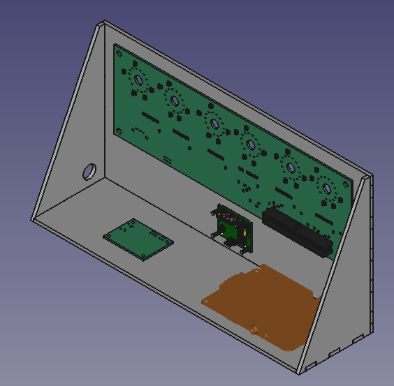
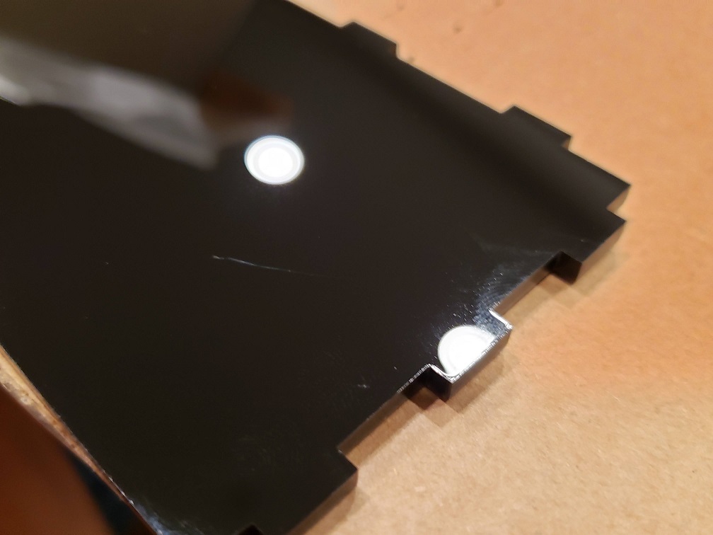
Since a laser cut enclosure is just a set of 2D shapes of fixed thickness, I could no longer have the small features I’d designed to hold the various boards in place. In order to deal with this, I added screw holes on the front face to hold up the main board and PIR sensor. I’m planning to have the screw heads on the front face, with the screws going through a small spacer, the boards, and then a nut on the other side. I have no plans for securing the RPi and supply boards to the bottom of the enclosure for now, but I might make a ledge or something like that on a future revision. Note the hole on the right side for a button!
I like the look of this “open air” enclosure for a prototype, so I might keep that going forward. My main concern for now is that the whole thing is going to want to tilt forwards as it’ll be top heavy because of the tubes. I may have to increase the size of the base or make it heavier going forward. For now I can always weight it down with something.
2D view of the enclosure that I sent out to the manufacturer earlier today


")
")


")
")
")